
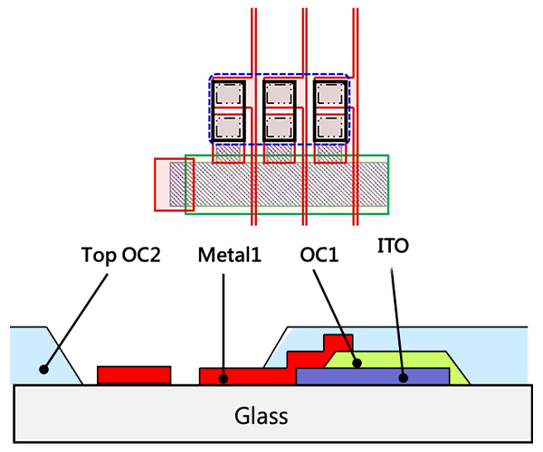
Micro LED glass backplane: Using multi-layer sputtering materials (ITO/Ti/Cu...etc.),and matching with photo/etching process. Covered protective layer OC material.
To make the LED glass substrate required for customer applications.
The sputter and photo materials required for its multi-layer structure can be designed according to customer needs.
The relevant characteristics are as follows:
1.The maximum glass size of the photo/etching process: (G2.5) 400x520x(0.1~2.9)mm.
2. Optical and graphic design: can be adjusted according to customer needs.
3. providing small amount of various products and services.
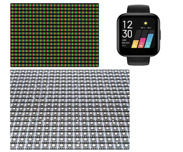
Micro LED, self-illuminating LED in nano-size, is believed to be the next generation display technology which will be widely used across the industries. Buwon is working with leading Micro LED players to develop Micro LED glass substrate by leveraging its stable sputtering and photo-etching technology.
Micro LED glass backplane: Size reduced to a micron level that is difficult to discern with the naked eye. By collaging LED chips of different RGB into a pixel, it can replace the color filter and LCD, which directly provides high-resolution images, is regarded as the next-generation display technology by the industry, and will be more widely used in various displays in the future.
With its stable sputtering and patterning technology, and with related Micro LED factories, Buwon has done long-term development and design, which will be used for more products in the future.